Semiconductor chips are arranged for a photograph on the production line at the Hana Microelectronics plant at the Hi-Tech Industrial Estate in Bang Pa-In, Ayutthaya province, Thailand, on Tuesday, April 22, 2014. (Dario Pignatelli/Bloomberg)
The U.S. Commerce Department is launching a $3 billion program to stimulate the domestic chip-packaging industry, a key link in the semiconductor supply chain that Washington worries has become dominated by Asia.
The packaging program is the first major research and development investment from the 2022 Chips and Science Act, which aims to revive semiconductor production in the U.S. as the development of critical electronic components has become a geopolitical battleground between the U.S. and China.
The funds for the effort, officially known as the National Advanced Packaging Manufacturing Program, come from $11 billion in the Chips Act earmarked for research and development, which is separate from a pool of manufacturing incentives worth $100 billion.
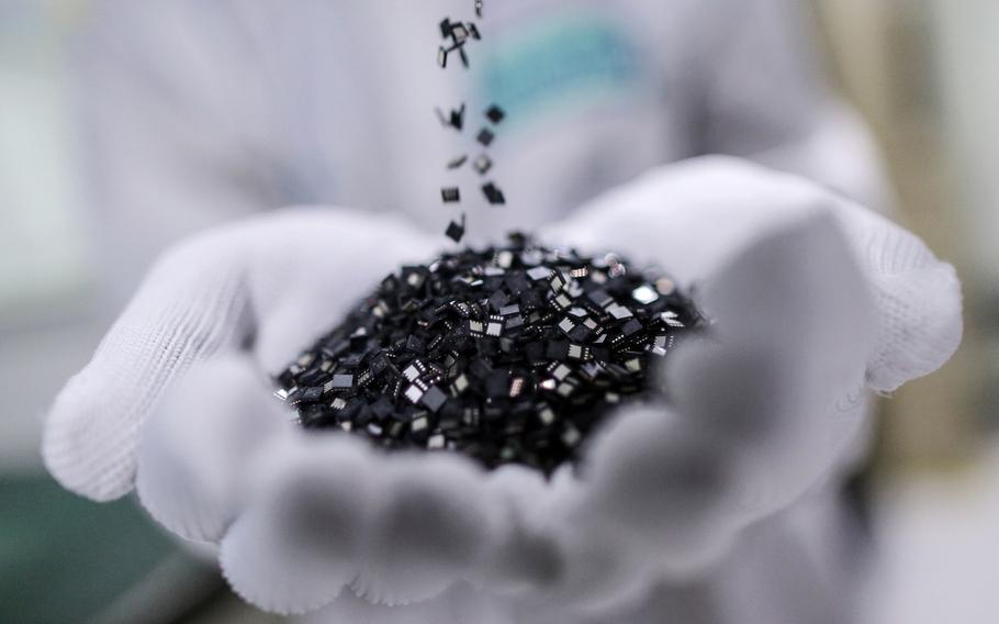
Packaging refers to the process of putting together individual chips for use in commercial products like phones and cars, as well as military applications including nuclear missiles. The Commerce Department says the U.S. has just 3% of the world’s packaging capacity — compared with an estimated 38% in China — which Washington worries has left the country vulnerable.
“Fabricating chips in America but then shipping them overseas to be packaged creates supply chain and national security risks that we just can’t accept,” Under Secretary of Commerce Laurie Locascio said Monday at an event at Morgan State University in Baltimore, Md., to unveil the effort.
By the end of the decade, Locascio said, the U.S. “will be home to multiple high-volume advanced packaging facilities, and a global leader in commercial-scale advanced packaging for the most sophisticated chips.”
The agency will release the first funding opportunity for packaging, focused on materials and substrates, in early 2024, Locascio said. Future investments will focus on other packaging technologies as well as the broader design ecosystem.
South Korean chipmaker SK Hynix Inc. has said it will invest $15 billion in a U.S. advanced packaging facility, and Arizona Gov. Katie Hobbs said that the state is in talks with industry leader Taiwan Semiconductor Manufacturing Co. about adding packaging capabilities at its $40 billion Phoenix project.
Arizona is in the “middle stages” of conversations with multiple global packaging companies and testing and quality assurance firms, said Chris Camacho, chief executive officer of the Greater Phoenix Economic Council, declining to comment on which firms are involved. He said he anticipates that companies could break ground on construction sites in 2024.
The Commerce Department’s packaging program will also establish an Advanced Packaging Piloting Facility, which aims to develop packaging technologies that can be scaled for U.S. production, as well as invest in workforce training.